Solar Cell Wafer Size

From M0 To M12 Different Wafer Sizes In The Market Ibc Solar Blog

From M0 To M12 Different Wafer Sizes In The Market Ibc Solar Blog

Longi 6 Others Propose M10 Wafer Size As Pv Industry Standard Clean Future

Longi 6 Others Propose M10 Wafer Size As Pv Industry Standard Clean Future

Pv Tech Talk Aiko Solar S Vice General Manager Michael Ho Pv Tech

Pv Tech Talk Aiko Solar S Vice General Manager Michael Ho Pv Tech

Two Types Of Silicon Wafers For Solar Cells A 156 Mm Monocrystalline Download Scientific Diagram

Two Types Of Silicon Wafers For Solar Cells A 156 Mm Monocrystalline Download Scientific Diagram

Longi Solar Explaining The Larger Size Of Mono Silicon Wafers

Longi Solar Explaining The Larger Size Of Mono Silicon Wafers

2bb 3bb 4bb 156mm 156mm High Efficiency Solar Cell Solar Wafers View High Efficiency Solar Cell For Sale Sr Solar Product Details From Shenzhen Sopray Solar Energy Technology Co Ltd On Alibaba Com

2bb 3bb 4bb 156mm 156mm High Efficiency Solar Cell Solar Wafers View High Efficiency Solar Cell For Sale Sr Solar Product Details From Shenzhen Sopray Solar Energy Technology Co Ltd On Alibaba Com

2bb 3bb 4bb 156mm 156mm High Efficiency Solar Cell Solar Wafers View High Efficiency Solar Cell For Sale Sr Solar Product Details From Shenzhen Sopray Solar Energy Technology Co Ltd On Alibaba Com

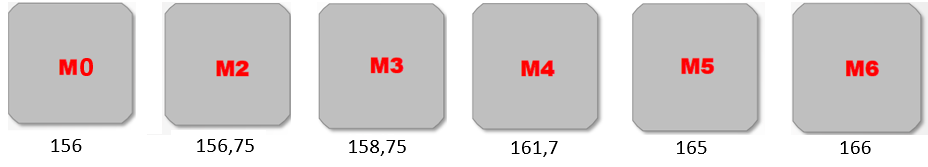
However leading mono wafer producer longi green energy technology and major merchant solar cell producers aiko solar and tongwei group started offering 161 75mm x 161 75mm.

Solar cell wafer size.

Multiple solar cells in an integrated group all oriented in one plane constitute a solar photovoltaic panel or module photovoltaic modules often have a sheet of glass on the sun facing side allowing light to pass while protecting the semiconductor wafers solar cells are usually connected in series creating additive voltage and current. At the end of q3 2019 longi solar the world s largest mono wafer manufacturer launched another variant on the market for the first time. It undergoes many microfabrication processes such as doping ion. Tim to 2019 m6 166mm x 166mm p type mono wafers 223mm diameter silicon ingot was lauched.

The 6 format m2 156 75mm x 156 75mm was expected to be placed by g1 and m6. However several manufacturers had their own ideas on what the larger wafer size should be such. In electronics a wafer also called a slice or substrate is a thin slice of semiconductor such as a crystalline silicon c si used for the fabrication of integrated circuits and in photovoltaics to manufacture solar cells the wafer serves as the substrate for microelectronic devices built in and upon the wafer. Changing the wafer size and moving to half cut cells was seen as the best option to get to 400wp.

Large area wafers of.

Pce Increase Of Hjt Single Wafer Solar Cell During The Development In Download Scientific Diagram

Pce Increase Of Hjt Single Wafer Solar Cell During The Development In Download Scientific Diagram

What Is Pseudo Square Diameter And Why We Should Know About It Solar Edition

What Is Pseudo Square Diameter And Why We Should Know About It Solar Edition

Pv Manufacturing Org

Pv Manufacturing Org

Risen Energy Announces 500w Hjt Module Taiyangnews

Risen Energy Announces 500w Hjt Module Taiyangnews

Source : pinterest.com